event [Nov 2025] We update arXiv version of our paper based on the feedback from queries and conferences. We highly recommend the curious audience to check out the updated version as it provides more explicit analysis results for our method.
event [Oct 2023] The paper got accepted to
SIGGRAPH
Asia 2023!
Abstract
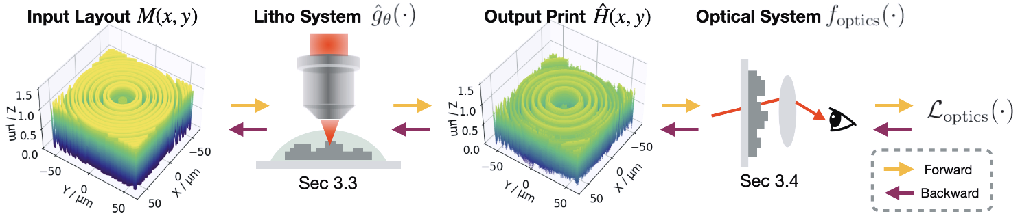
We introduce neural lithography to address the 'design-to-manufacturing' gap in computational
optics. Computational optics with large design degrees of freedom enable advanced functionalities
and performance beyond traditional optics. However, the existing design approaches often overlook
the numerical modeling of the manufacturing process, which can result in significant performance
deviation between the design and the fabricated optics. To bridge this gap, we, for the first time,
propose a fully differentiable design framework that integrates a pre-trained photolithography
simulator into the model-based optical design loop. Leveraging a blend of physics-informed modeling
and data-driven training using experimentally collected datasets, our photolithography simulator
serves as a regularizer on fabrication feasibility during design, compensating for structure
discrepancies introduced in the lithography process. We demonstrate the effectiveness of our
approach through two typical tasks in computational optics, where we design and fabricate a
holographic optical element (HOE) and a multi-level diffractive lens (MDL) using a two-photon
lithography system, showcasing improved optical performance on the task-specific metrics.
TL;DR: A real2sim pipeline to quantitatively construct a high-fidelity neural photolithography
simulator and a design-fabrication co-optimization framework to bridge the design-to-manufacturing gap in
computational optics.
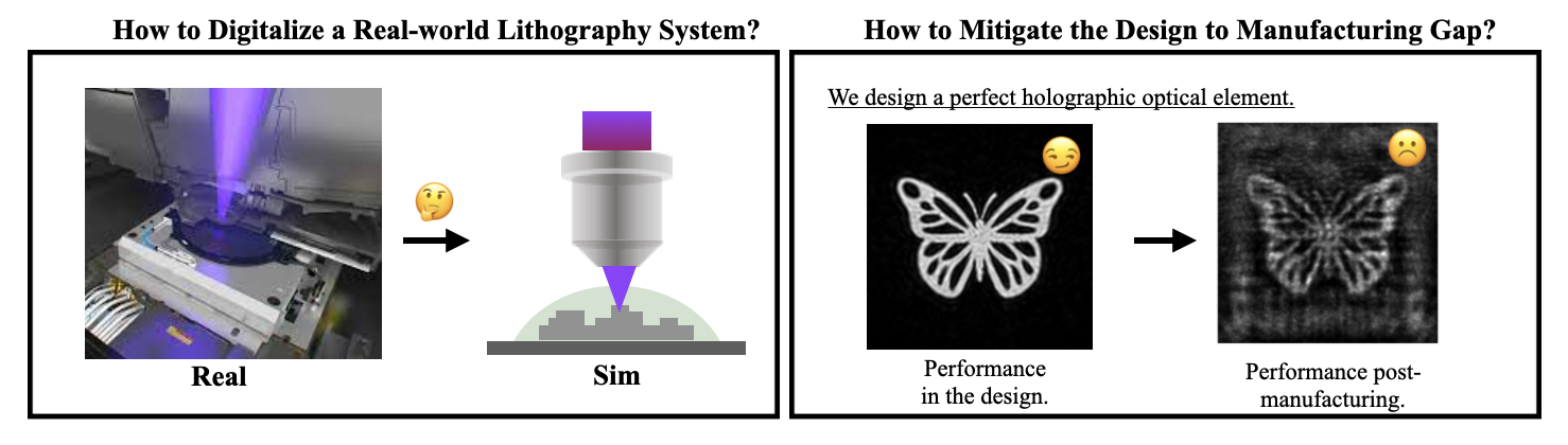
This work identifies two obstacles in computational optics:
1⃣ What is the "elephant in the room" in Computational Lithography?
- High-fidelity photolithography simulator | "No matter how good we can advance the computational
(inverse) lithography algorithm, the performance bound is grounded in the fidelity of the lithography
simulator."
2⃣ What hinders the progress of computational optics?
- One should be the Design to Manufacturing gap. |
"Yes you can design a perfect lens, but you cannot guarantee the post-manufacturing performance."
Accordingly, our work tackles the above questions and opens up two exciting research directions:
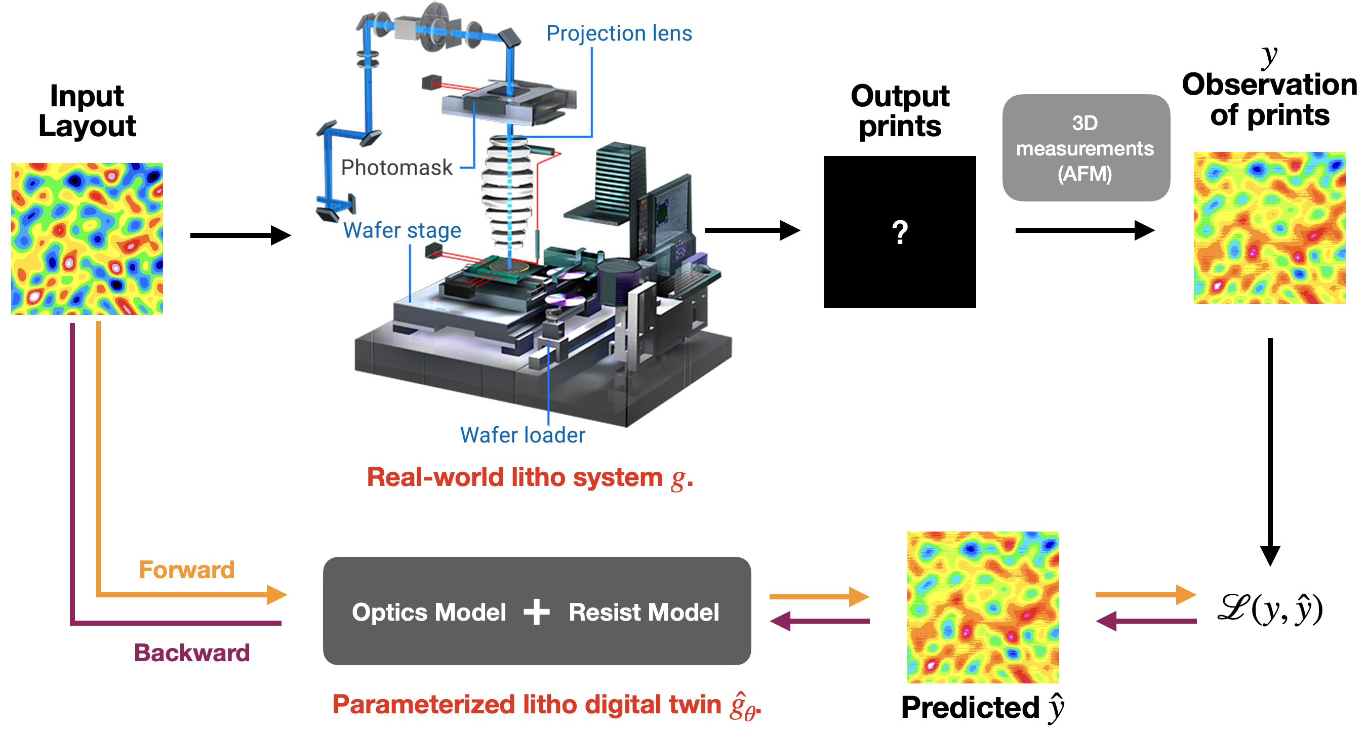
1⃣ Real2Sim learning for 3D modelling the fabrication outcome of any real-world photolithography
system.
Pipeline to digitalize the lithography system through the real-world measurements.
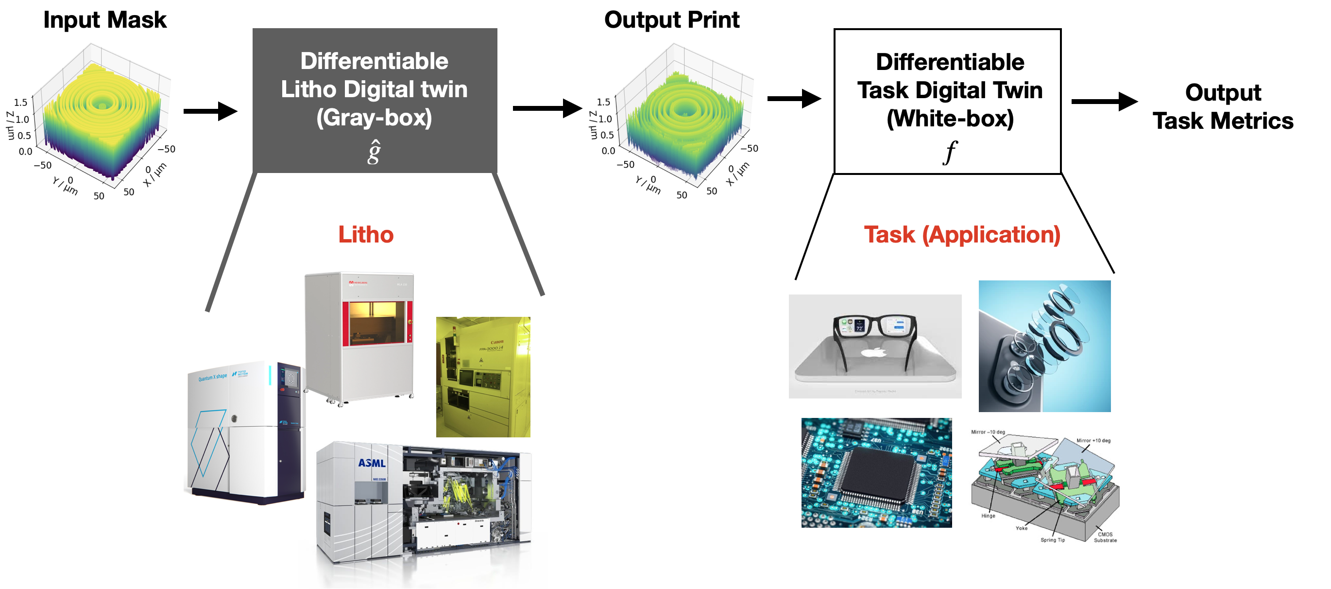
2⃣ Close the Design-to-manfuctuting gap via co-optimizing the manufacturiability and the task design
with two intersected differentiable simulators (Litho + Task; DTCO).
Design Technology (Manufacturiability) Co-optimization (DTCO) through chained
differentiable simulators.
Some Results (Expand it if you want to see the results)
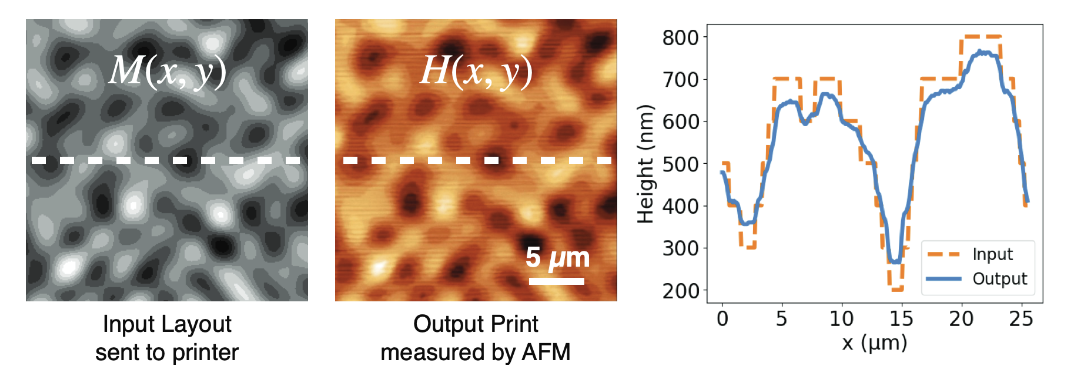
Learn the lithography system.
We experimentally collect a dataset to learn the neural lithography simulator.
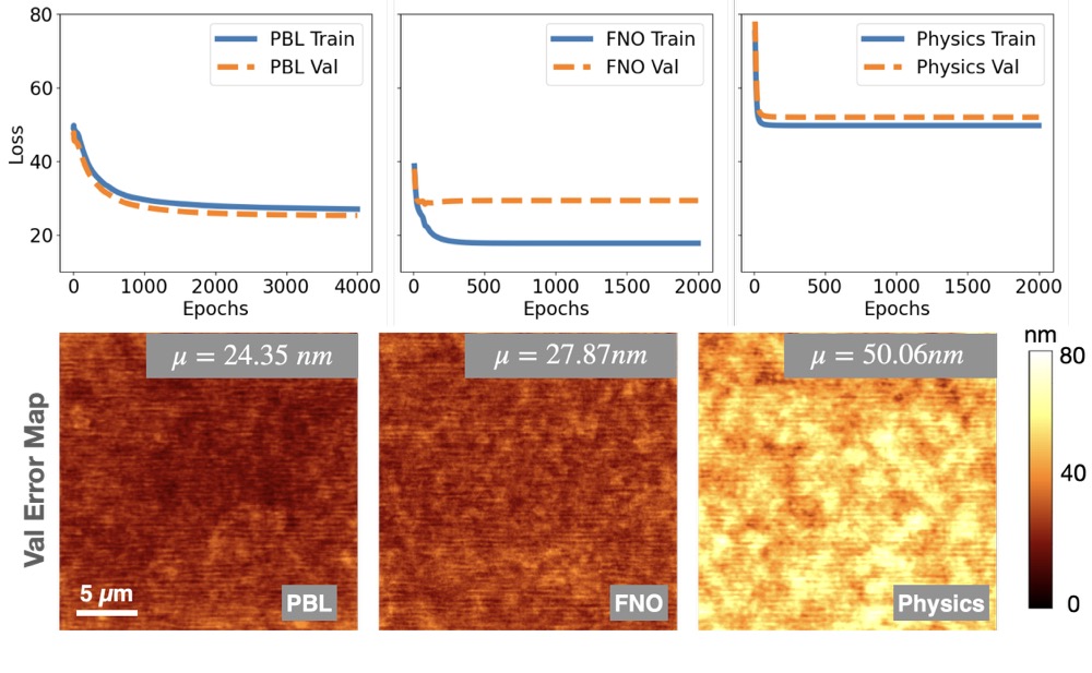
Predicting capability of the learned neural lithography simulator on three models we
explored in neural lithography. The PBL (see details in the paper) performs the best
and thus is used throughout the paper. Top: The training and validation loss
curves correspond to the three models explored in our work. Bottom: The corresponding
average validation error map and the mean error value across the map.
Mitigate the design to manufacturing gap.
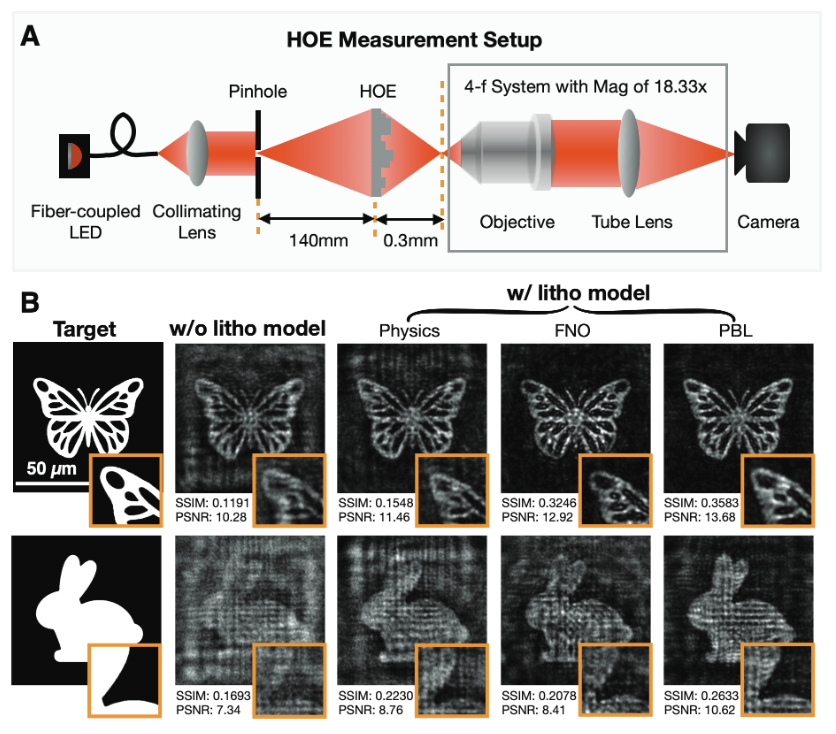
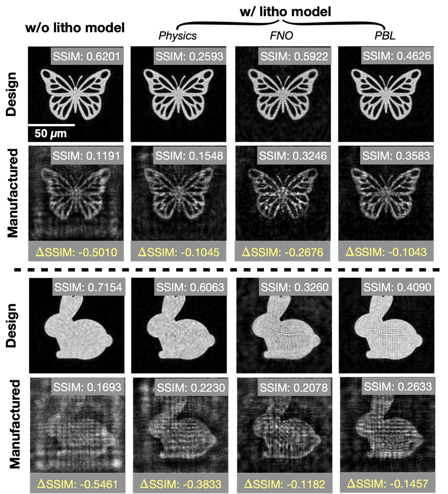
Results on holographic optical elements.
We show improvement in performance when design the holographic optical elements(HOE)
w/ our learned litho model.
We quantitatively show improvement in performance when design the holographic
optical elements(HOE) w/ our learned litho model.
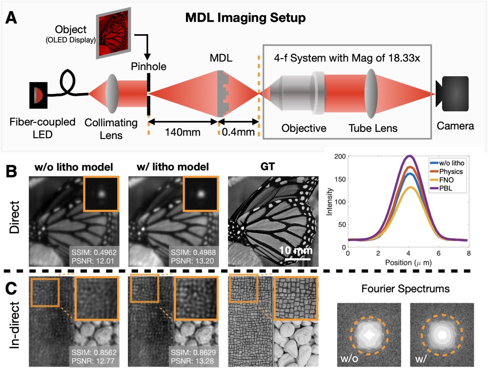
Results on multi-level diffractive lenses which can be used in direct and computational imaging.
Imaging performance with the designed MDL. A: Sketch of the setup for
characterizing the performance of MDL. B: We show our measured PSFs and direct
imaging results (i.e., w/o deconvolution) corresponding to design w/o and w/ PBL
litho model. The end of this row shows the line profiles of PSFs designed w/o or w/
different litho models. C: Computational/Indirect Imaging result of the MDL. The
lower right compares the Fourier spectrum of the designed PSFs. Our method's
design enhances the contrast in direct imaging (B) and the high-frequency
imaging performance in computational imaging (C).
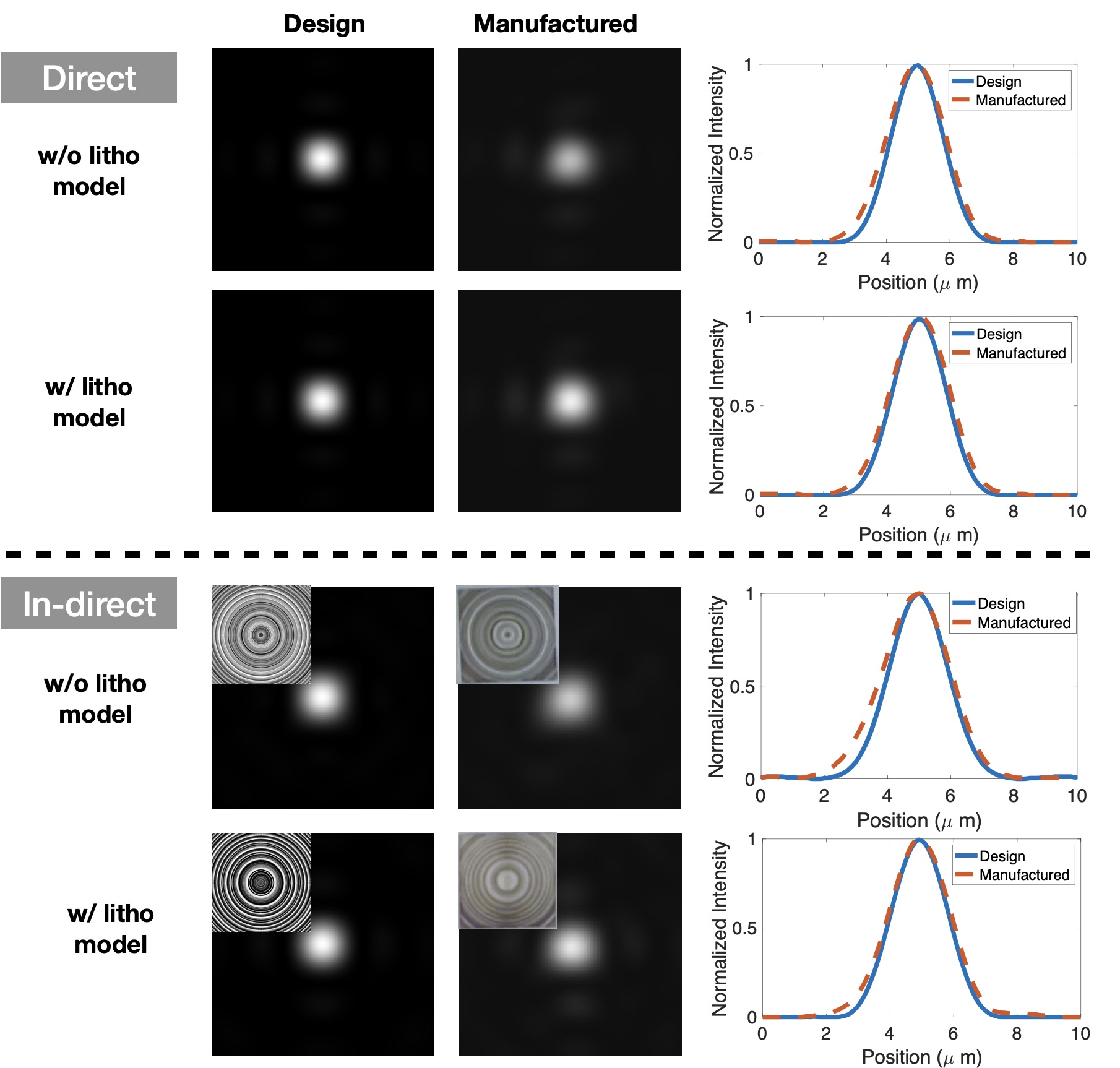
Comparison of PSFs generated by MDLs in the design and real experiment. In
both the direct and indirect/computational imaging setting, the naive design w/o
lithography model has a larger deviation between the shape from the designed and
experimental PSF. In contrast, the deviation is small when we apply neural
lithography.
Frequently asked questions (FAQ)
1. Does this work provide a 'one-size-fits-all' litho model?
NO. Our goal isn't to learn a model that generalizes across different lithography types or
different modalities of a type. Instead, we present a pipeline on how to OVERFIT to a single lithography
system with a specific photoresist and post-processing procedure.
2. What are the assumptions for the applicability of the learned neural litho model?
1⃣ No single lithography process can be perfectly represented by one white-box model. Factors like
optical misalignment, hardware tolerances, differences in conditions, and even temperature and humidity
can introduce variability.
2⃣ If a specific lithography system and photoresist remain consistent over time, and once digitalized
remain stable, a learned gray-box simulator trained on data from that environment should be effective.
3. Did this work included the pure differentiable physics based fabrication (lithography) model or just a neural network?
Yes we not only have neural lithography model but also included another pure differentiable physics based fabrication (lithography) model in our work. The Neural Litho simulator is a more complete version that includes the physics-based model and neural network to learn the residuals and we demonstrate the pure differentiable physics based fabrication (lithography) is inferior to the Neural Litho simulator which combines the best of the two worlds.
4. Why use AFM but not SEM, as AFM is not precise for measuring 2.5D height maps at ~10nm scale?
It is true that for some AFM modalities such as what is used in our work, the height precision is not as fine as sub-nanometers. However, the SEM cannot get you any height profiles and as a result the height error for SEM is +∞. Thus, we believe the more information, the better outcome and choose the best of the worst as a comprise for now.
5. What is the difference between the SA'23 paper and the arXiv version?
The arXiv version is more comprehensive and contains more details and it will be updated while the SA'23 paper is published and will not be updated anymore. Moreover, the arXiv version has no page limit and we merge useful information from supplementary materials into the main paper.
Citation
@article{zheng2023neural,
title={Neural Lithography: Close the Design-to-Manufacturing Gap in Computational Optics with a'Real2Sim'Learned Photolithography Simulator},
author={Zheng, Cheng and Zhao, Guangyuan and So, Peter TC},
journal={arXiv preprint arXiv:2309.17343},
year={2023}
}
@inproceedings{zheng2023close,
title={Close the Design-to-Manufacturing Gap in Computational Optics with a'Real2Sim'Learned Two-Photon Neural Lithography Simulator},
author={Zheng, Cheng and Zhao, Guangyuan and So, Peter},
booktitle={SIGGRAPH Asia 2023 Conference Papers},
pages={1--9},
year={2023}
}